Signal Integrity R&D and Support

As signal data
rates continue to rise, connector manufacturers must continually evaluate their
manufacturing processes and product offerings to ensure they continue to
provide reliable products while meeting the market demands. High reliability
connectors will always be a cornerstone for Omnetics, but for many
applications, a robust mechanical design must be balanced with a solution that
is also optimized for high-speed. In order to achieve this, many aspects of the
design – material selection, connector spacing, termination strategy, and
cabling – must be constantly under evaluation. Omnetics uses a combination of
software and hardware to address these challenges.
For design
optimization, Omnetics uses ANSYS HFSS, a 3D Electromagnetics simulation tool,
to simulate and optimize the performance of their products. This allows Omnetics to quantify the impact
of various design options prior to manufacturing, helping to constantly improve
products and find ways to maximize the data rates of any given solution.
For
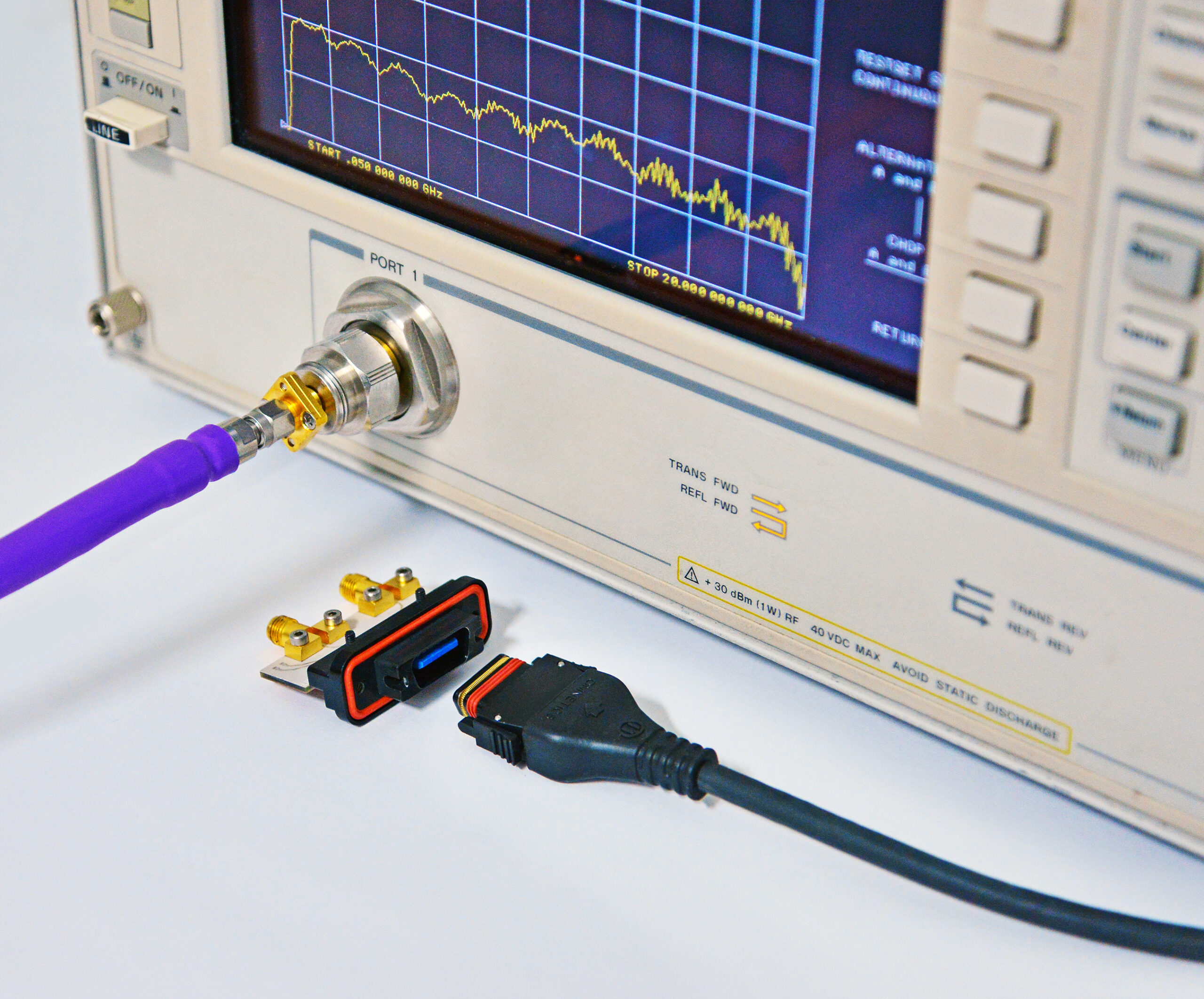
characterization and verification, Omnetics has an in-house Signal Integrity
Lab that is equipped with state-of-the-art testing equipment, including a
4-port Keysight PNA with Keysight PLTS for post-processing analysis. This provides
the ability to characterize and verify the performance of all Omnetics products,
as well as provide production testing for impedance upon request.
Omnetics
prides itself on providing accurate and reliable signal integrity data for all applications. Test reports are available for many
configurations. Additionally, S-parameter models (whether it’s from simulation
or measurement) are available upon request. Customs designs can even be models
and simulated to to provide S-parameter models that are specific to your
applications.
